| To Part Two
In Cheap Outboards, Max Wawrzyniak warns us that electronic ignition is not worth messing with. I knew he was right. Really! But you know how I am about these things. I have to at least try to fix it, even when it’s not a good idea. Especially if it seems like a bargain!
And so it was for this project.
This project is actually a snowmobile, but the principles are identical to those on an outboard motor. After all, this is still two cylinders, two strokes and two sparks – well, in this case no spark. The machine is question is an early 1970s Rupp American 40 hp with a Tohatsu engine. If you can actually find a CDI box for this motor, it will cost well over $100. I paid $75 for the whole machine! (…and now I know why!)
But I couldn’t walk away easily. There was a visible broken wire on the ignition box. If I could only get that connected…
Man, if I had a dollar for every time I said “if only” and it turned into a huge project. Before you read any further, be advised that this article isn’t really a “how-to”. It’s a “when-not-to”. So beware—I take you on a rather long trip through an attempted repair that was ultimately futile.
Still reading? OK, you were warned. Let’s have a look inside.
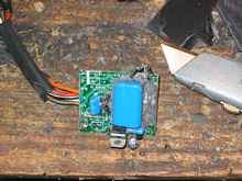
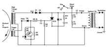
Inside the CDI
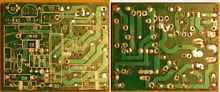
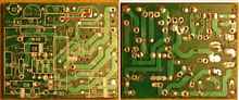
First we remove the plastic case with some careful hacksawing and prying. In this case the inside is filled with toxic-smelling dense foam, but often it is silicone sealant. So we carefully slice away all this filler with a razor. Take thin shavings and stop if you meet resistance – it’s probably the board or a component. I could have stopped when I got to the broken wire, but I wanted to come up with a schematic so I could build a backup unit to have on hand. (This was a warning sign that things were getting out of hand. I should learn to notice them.)
There is no good reason for the foam filler, by the way. They use it in partly as a cheap way to deaden vibration and partly to make it harder to reverse-engineer things like we’re doing.
This slicing is fiddly work. Do not be tempted to use acetone do dissolve this foam. It probably will, but it will also dissolve the markings on the components! Those markings are what we really need, since the components are cheap. Thus, I didn’t worry too much about breaking a couple component leads. (This turned out to be a bad idea.)
Fortunately my acetone attempt only melted resistor codes, and those values are easily measured. They could also be unsoldered and read on the good side.
Components
For those who are new to electronics, let’s look at what these components do and how to identify them. Actually I’d better provide a brief glossary:
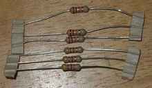
Resistors
In electronics we often use plumbing analogies. Voltage is like water pressure, and current is volume of flow. Resistors are like narrow spots in the pipe that restrict the flow and resist the movement of the current.
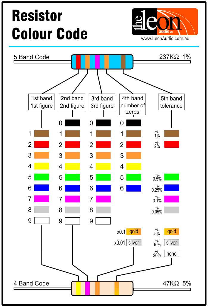
Resistors are easy to figure out. A resistor color code index can be found here: https://wiki.xtronics.com/index.php/Resistor_Codes and https://www.leonaudio.com.au/res-code.gif, as well as many other places on the web.
I’m guessing the larger ones are ½ watt and the smaller are ¼ watt. The percentages are tolerances, but resistors are really cheap, so I always buy 5% or smaller tolerances.
I measured all of these resistors with a multi-tester as well as reading the color code. Sometimes the colors are faded and hard to discern with certainty—orange can look like brown, violet like red, etc.
Our resistors are:
R1 = brown-black-green-gold = 1M (1 megaohm, or 1,000,000 ohms), 5%
R5 = brown-tan-purple-gold = 180M, 5%.
Meter says 178.7 ohms! 180 ohms should be brown-gray-brown. I guess that purple was really brown and the tan was gray. (There is no tan in the code system.)
R6 = brown-gray-brown-gold = 180 ohms, 5%.
Meter says 178.7 ohms. Aha, the colors looked right on this one.
R7 = brown-black-black-gold = 10 ohm, 5%
R8 = orange-black-black = 30 ohm, 20%
R9 = yellow-purple-black-gold = 47 ohm, 5%
R10 = red-black-black-gold = 20 ohm, 5%
S1 = brown-black-green-gold = 1M, 5%
That last one is a resistor in a spot meant for a transistor. I guess this board was designed to serve in a number of different circuits, which undoubtedly kept production costs down. I got all ½ watt resistors because it seemed safer to stick with a 400 volt rating, and all of these happened to be ½ watt.
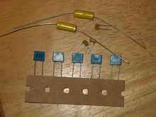
Capacitors
Continuing the plumbing analogy, capacitors are like surge tanks, which tend to prevent large fluctuations in voltage.
Sometimes we see this kind – electrolytic capacitors. They are the same deal, except they’re polarized, which means you can put them in backwards. These are most commonly seen in power supplies for smoothing out the 60 Hz noise from rectified AC power.
Anyway, capacitors are similarly easy: https://wiki.xtronics.com/index.php/Capacitor_codes
The big cap is marked “Mitsuko 2G255 G921”. Well, the first bit is the manufacturer. I’m not sure what the “2” is all about, but the “G” tells us 2% tolerance and the “225” tells us “22 plus 5 zeros”, or 2,200,000 picofarads (pF), which is more commonly known as 2.2 microfarads (uF).
We also need to know the voltage rating. I couldn’t make any sense of “G921” as a voltage rating. They normally will simply say something like “630 vdc” (vdc=volts direct current). But often mass-produced circuits are made with oddly labeled components they bought in bulk or had custom manufactured.
I got around this by simply looking for a cap of the same value and composition that was about the same physical size. This isn’t as haphazard as it sounds – manufacturers are always trying to use the least material possible to get a given rating and value, so sizes are pretty consistent for a cap of same material. Mouser Electronics (www.mouser.com) is great here, as they have a searchable online database with relatively handy filter options. I’m guessing polyester film. This cap is around 30x20x9 mm. Looking at a few representative datasheets (such as https://www.cde.com/catalogs/DME.pdf) I’m guessing we’re in the neighborhood of 250 or maybe 400 vdc. A higher voltage tolerance never hurts, however, and we won’t be constrained by the original box or mass production budget anymore. Since I broke one of the cap’s leads I’ll replace it with 400 vdc or more. A 400v cap will cost around $2.80, and the only larger readily-available option is 630v for $6.00. This one is huge at 31x29x20 mm, so 400 volts is probably plenty.
The smaller cap is .1 uF. It is still in tact, so I won’t need to replace it. But if I had to guess its voltage rating, I would again look at the size. At 12x8x4 mm, I would guess about 250-400 vdc, again. I’d replace with 400 vdc.
Important caveat: this is not a great way of guessing voltage ratings. Keep your face well clear when you first operate the device, and keep something between you and anything you care about. If one of those caps blows up, it can fail sliently or sound like a shotgun and throw smoking bits of plastic everywhere. Over-engineering the voltage ratings tend to prevent this.
Now we move on to the semiconductors.
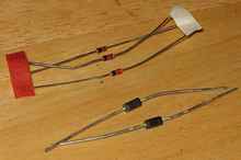
Diodes
A diode is like a check valve – it only lets current flow one way. The arrow in the symbol points in the direction current can flow, and we call in ingoing side the anode and the outgoing side the cathode.
Our diodes are all marked “FR207”. Mouser’s search function takes us right to it! They are 1000 volt, 2 amp fast recovery rectifiers. They only cost 18¢ each, but that is expensive for a diode. Worse, you can only get them in rolls of 500! However searching by “fast recovery rectifier 1000v 2a” yielded a device available singly for 60¢ each. That would come to $3 worth of diodes for this device if I were starting from scratch.
We also need a zener diode. I broke this one in half, but managed to read the markings with strong magnification and bright light. Sort of. It was 0ZX or ZX, then 550 or 530, and a Q or a 0. Or maybe that last one was part of the stripe. Searches on Mouser and Google came up short, but the Mouser database let me try to narrow in. Of 2,960 zener diodes, only 614 has axial leads. A search within these results for “530” yielded no results, but “550” got it down to 11 results. But none with anything like the part number on this device.
Sooo…now we need to do some actual engineering to figure out what to use. A zener diode is normally used for circuit protection or voltage regulation. It normally acts like a regular diode – a check valve. But when the pressure on the downstream side gets too high it opens up and acts as a pressure relief. So a zener diode to ground normally does nothing at all, but voltage spikes that could damage other components get shunted to ground. Cool, huh? This can also be used to regulate voltage. When we get to the schematic, we’ll see what this zener is doing. The markings on this diode didn’t yield anything useful, so it’s probably a proprietary part. Fortunately the only real variables are voltage and current ratings.
Well, that takes care of the two-lead semiconductors. On to transistors.
Transistors and similar
Here things get trickier. These devices are like valves that are remote controlled by water pressure. The arrow points in the direction of the main current flow, and it flows from anode to cathode, just like with the diode. However, for transistors these are often called collector and emitter, respectively. The middle one is the control, called the base.
The big transistor with the heat sink hole on it is marked “MRC TYN 412”. This yielded nothing, so I took off the MRC, which is probably the manufacturer. Here we get something. It’s a SCR, or silicon controlled rectifier rated at 12 amps and 400 volts. They cost $1.04 each, which is about 20x what a transistor of the same size costs. A SCR is a lot like a transistor, except we call the base a gate. The difference is function is that it stays on once you turn it on, even if the gate current stops. It stays on until it has emptied the “pipe” leading to its anode. This is used in the power switches on high-end stationary power tools. Press the start button to start it and it stays on, but if the power fails, it turns itself off, so it won’t re-start unexpectedly when the power comes on.

[Does not enlarge] |
(Note that these look exactly like power transistors, unless you read the markings.)
The small transistor required powerful magnification and excellent lighting to decipher that it was marked “XL02 ST 40 T955”. The “ST” is the manufacturer’s logo, and corresponds to ST Microelectronics (www.st.com). They provide a part number search, but this one didn’t come up. I had to create a login on ST’s site to pose my question to technical support. They said that it is a non-standard part number, thus a proprietary part they made for someone, so they cannot release technical data. This is frustrating, since there is probably nothing exotic about the transistor. In fact, it is entirely likely to be a component they ordered a boatload of for some other product that didn’t sell, so they designed this circuit to use what they had.
(There are SCRs that look like this too, if they are made for signal-level applications)
If we knew which lead is which we could try some common ones to see what happens. Some good instructions for this can be found at https://www.allaboutcircuits.com/vol_3/chpt_4/3.html. Unfortunately this transistor had partially failed. With only one side working there is no way to figure out its configuration. This means we need to resort to actually knowing what’s going on. (Don’t you just hate that?) We’ll get back to that in the circuit analysis below, but first we need to figure out the basic connections.
But it is some comfort that there was more wrong than just the wire. I would have ended up cutting away that foam anyhow.
Thoughts on Circuit Tracing
This is really just a simple matter of making a diagram of how everything links together. By convention it is common to start with the active device (transistor) and draw it “pointing” downward. Literally, the arrow part of the symbol usually points downward! The anode is the source side and the cathode is the designation side. Then circuit is generally shown as more or less “proceeding” left to right, when possible.
If you want to figure this out with the components in place, you will probably need a good ohm meter, as well as an understanding of Ohm’s Law and voltage division. Sometimes traces run under components and you can’t see exactly where they go. This is especially true when everything has remnants of black foam on it! I find it easier to remove all the components. That way I could clean the board and get an unambiguous look at what went where. It also let me individually test components and replace any that were way out of spec.
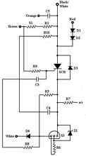
Fortunately this board is labeled with component numbers. Unfortunately they don’t always make sense. For example, D2 and D6 look like single diodes on the board, but they used two diodes in series to get the value they wanted. I assume this is because they couldn’t get the “right” component cheap enough, or they had on hand a whole lot of diodes that need doubling to work right. Further, some caps and resistors are missing, and components like S1 and S4 are resistors or jumpers. My guess is that “S” means “switch” (or transistor) in this case, and that the same board was used for many different CDI applications, with component changes to work with a given ignition system. We aren’t manufacturing these, so we don’t care about that. In fact, I will make a simplified board and leave all of that stuff out. We’ll get to that later.
The Labyrinth
OK, now that all the explanation is out of the way, let’s trace this thing. It’s a lot like doing a maze, and on a multi-application board like this you can ignore the dead ends. Just make sure they’re truly dead ends! Sometimes a solder-filled hole is used to connect to another trace the other side of the board.
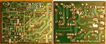
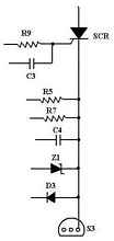
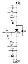
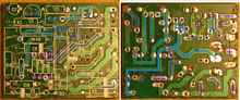
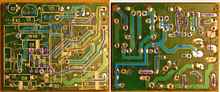
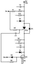
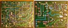
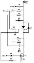
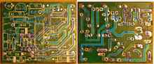
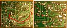
Here’s the clean PCB, front and back, and the back is reversed so it’s like we’re using our X-ray vision and looking through the top. (Otherwise we would have to mentally do a mirror image, and that is no fun at all.) Components were in the empty holes, but the filled-in holes always were filled in and may as well stay that way.
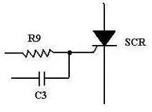
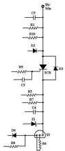
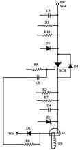
So let’s start with the SCR. The data sheet tells that we are looking at the cathode, anode and gate in that order from left to right.
This shows us that the gate connects to R9 and C3 in parallel. So we draw it into the schematic.
Now let’s look at the SCR cathode. I’m showing the current traces in red and traces we already accounted for in blue.
It connects in parallel to the cathode of the zener diode, the anode of D3, R5, R7, C4 and a terminal of the transistor. Unfortunately we really can’t be sure which terminal unless we know more about the transistor. So for now we will use a PCB-like transistor symbol rather than the typical schematic symbol.
Let’s finish up the SCR by tracing its anode.
It connects to the cathodes of D2 and D3, R10, R1, C5, and the external black/white wire. Now we start connecting to the other side of things we already have (D3).
Here I started adding crosses through the through-holes I had accounted for as well as tracing in purple the traces that aren’t connected to anything. Let’s also trace the other two connections to the transistor.
R6 connects between the two terminals, and the outer terminal connects also to the anode of D6 and R8.
The cathode D6 goes to the white wire off the board, and the other end of R8 connects to the free end of C3.
Now let’s finish R1. It connects to S1, and the other side of S1 connects to R9 and the two brown wires off the board.
It starts getting easier now. The free end of C5 connects to the orange wire off the board, and the free ends of R10 and C4 are connected. Perhaps most interestingly, R7 is unconnected at its other end, and thus serves no purpose in this circuit! A manufacturing error, I suppose.
Almost done. The anode of Z1 connects to R6 at the middle terminal of the transistor, so clearly it is meant to protect or control this component. The anode of D2 connects to the cathode of D1, and D1’s anode connects to the red wire off the board. And I missed the connection of R5 to the anode of D6, R8 and a transistor terminal.
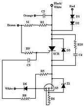
Now let’s clean up this schematic a bit. I eliminated R7 because it isn’t doing anything.
And let’s add the rest of the circuit outside this board. One brown and the orange go to spark coil primaries, blk/wht goes to the ignition switch and is grounded when off, and brown, red & white go to the primary coils on the stator. One of those coils is meant to charge up the capacitor, and the other provides the signal to tell the circuit to discharge it, thus creating the spark.
We clearly have a problem here. To discharge the big capacitor, the cathode of the SCR should be going to ground, and relatively directly. There’s no way this can work if it has to go to ground through the transistor circuit and the trigger coil. Time to have a look at the board again. Sure enough, I missed one of those through-board connections.
This yields a more reasonable schematic.
The configuration of the circuit with the zener diode is a guess. Given this and the unhelpful response about the smaller transistor, I guess that brings us to…
To be continued next month...
Rob Rohde-Szudy
*****

|


